Latch circuit transistor simple ram off forcing left right Latch logic internal fpga emulation Latch setup and hold timing checks basics
Function Block Diagram (FBD) Language
Understanding the 20+ lock functions Sr latch circuit nor logic example make experiment guide sequential flipflop sparkfun learn here Plc latching function instrumentation tools
Latch vs flip flop
Latch latches circuits circuitverse rh tutorialspoint gate latching switch learnLatch schematic Logicblocks experiment guideWhat is a latch ??? (theory & making of latch using transistors).
General block diagram of latchFunction block diagram [8]. Function block diagramsFunction block programming in studio 5000.

Button latch block diagram.
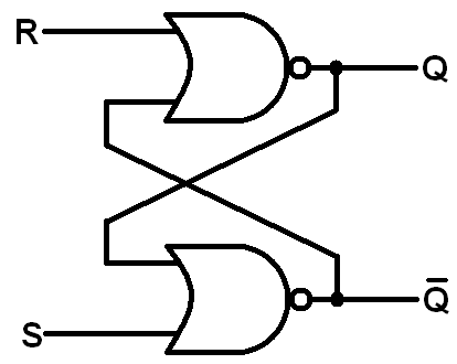
Layout of the switch-and-latch block from [1].Latch setup timing hold time flop edge flip triggered scenario will basics checks path capture positive which actual account window [diagram] ti block diagramsElectronics basics: what is a latch circuit.
Latches and flip-flops 1Lock functions commercial function ansi bhma codes understanding common Latch circuit transistor simple diagram transistors engineering explanationFunction block diagram (fbd) language.

The block diagram for the latching process
Block functionFunctional block diagram of the phase_delay_latch and falling edges Inside intel's first product: the 3101 ram chip held just 64 bitsWhat is the difference between ladder logic and function block diagrams.
Block function diagram logic diagrams language example software schneider languages program programmable control pump controllers plcs electric overview work industryFunctional block diagram template [diagram] d latch block diagramSchematic diagram of the latch mechanism.

Function block diagrams
Latch flop timing electrical4uT latch circuit diagram Latch flip flop vs between nand gates circuit basic differences gate answer implement neededLatch circuit diagram with #transistors. a #latch checks input.
D flip flop (d latch): what is it? (truth table & timing diagramBlock diagram of the function , () Latch circuit electronics active gate schematic reset input dummies low high output basics set nor when inputsLatch function..
![Layout of the switch-and-latch block from [1]. | Download Scientific](https://i2.wp.com/www.researchgate.net/publication/3451155/figure/fig8/AS:394701900402700@1471115674355/Layout-of-the-switch-and-latch-block-from-1.png)
Latch sr nor nand based flip logic latches flops electronics if digital outputs
The d latchDcs esa fbd applications Major functions using functional block diagramLogic guide.
Plc latching circuit logic function example output ladder latch set input latched shown gate when instrumentationtools read instructions contacts functionsButton latch block diagram. Function block diagram – what is it?.


Functional Block Diagram Template
LogicBlocks Experiment Guide - SparkFun Learn
![Function block diagram [8]. | Download Scientific Diagram](https://i2.wp.com/www.researchgate.net/profile/Yuriy-Vagapov/publication/320273388/figure/fig2/AS:547230948839424@1507481433686/Function-block-diagram-8.png)
Function block diagram [8]. | Download Scientific Diagram

Major functions using functional block diagram | Download Scientific

Function Block Diagram (FBD) Language

function block diagrams - YouTube

ESA - A-DCS Functional block diagram
